| 1. | ||
| 2. | ||
| 3. | ||
| 3.1. | ||
| 3.2. | ||
| 4. | ||
Tensoresistive Properties of Thin Polycrystalline (Bi0.3Sb0.7)2Te3 Films at Static and Cyclic Deformations
Shavkat Sh. Abdullaev, Nosirjon Kh. Yuldashev, Khusanboy M. Sulaymonov
Department of Physics, Ferghana Polytechnic Institute, Ferghana, Uzbekistan
Email address
 (N. Kh. Yuldashev)
 Citation
Shavkat Sh. Abdullaev, Nosirjon Kh. Yuldashev, Khusanboy M. Sulaymonov. Tensoresistive Properties of Thin Polycrystalline (Bi0.3Sb0.7)2Te3 Films at Static and Cyclic Deformations. International Journal of Modern Physics and Application. Vol. 3, No. 4, 2016, pp. 52-56.
Abstract
The tensoresistive properties of polycrystalline (Bi0.3Sb0.7)2Te3 films at static and cyclic deformations have been investigated. It is shown that the linear portion of the current‒voltage characteristic expands from (0; 5) V (at N=0) to (0; 12) V for the films subjected to N=5×10⁵ deformation cycles. The temperature coefficient of resistance in the range of 293 K - Tmin changes from a=-5.6×10⁻³ K-1 to a=-2.5×10⁻⁴ K-1. The value Tmin, at which a=0, increases with an increase in N. Tensoresistive (Bi0.3Sb0.7)2Te3 films can successfully be used in fatigue stress accumulation sensors in the temperature range T=273-413 K for a number of cycles in the range of N=0-5×10⁵.
Keywords
Polycrystalline Composite Film, Border of Grains, Internal Mechanical Pressures, Static Deformation Characteristic, Alternating Stress Cycles, Fatigue Damage Accumulation
1. Introduction
The tensoresistive method is one of the most widespread and informative techniques for studying the deformation properties of thin-film strain gauges, which are widely applied as electric sensors [2, 2] and fatigue damage accumulation (FDA) sensors [3‒6]. When thin semiconductor films are intended to be used as strain-sensitive elements, their current‒voltage (I‒V) characteristic yields information about the power parameters of resistance strain gauges. An important parameter is the maximum allowable power of resistance strain gauge under specified operation conditions. The reason is that semiconductor films are very sensitive to illumination and variations in temperature. High currents through film samples may cause extra Joule heating and, correspondingly, affect their working parameters. In particular, this heating makes the I‒V characteristic nonlinear, thus increasing the measurement error. In this paper, we report the results of studying the influence of static strains and alternating stress cycles (ASCs) on the I‒V characteristic and the temperature dependence of the resistance of tensoresistive (BixSb1-x)2Te3 films. This information is necessary for designing FDA sensors based on these films.
2. Measurement Technique
Polycrystalline (BixSb1-x)2Te3 films with an area of 5x20 mm were obtained by thermal evaporation in vacuum with a residual vapor pressure of (1-3)×10-2 Pa from a mixture of Bi2Te3 and Sb2Te3 powders in a ratio of x:(1-x) mol %. The substrate (polyamide PM-1) temperature was varied in the range Ts=323-423 K, and the film growth rate was W=150-450 Å/s. The most strain-sensitive (K=ΔR/(R0×ε) »103 rel. units - where ε is the relative strain, R0 is the film resistance at ε = 0, and ΔR= R(ε)–R0) films had thicknesses d»3-5 mm and were obtained at Ts=363, W=200 Å/s, and x=0.3. The strain characteristics of the films were measured using the same technique as in [3, 7-10]. No preliminary thermal treatment was performed. The as-prepared films had an unstable strain sensitivity coefficient (SSC, K), caused by the presence of significant nonequilibrium internal mechanical stress. With an increase in the number N of ASCs, the K value monotonically decreases; this behavior indicates to the potential of these films as FDA sensors. Electron microscopy and X-ray diffraction study [3, 7] showed that the grown (Bi0.3Sb0.7)2Te3 layers have a polycrystalline columnar porous structure. The sizes of individual crystallites are 1.0-1.5 mm.
3. Experimental Results and Discussion
3.1. Influence of Static Strain and ASCs on the I-V Characteristics of Films
The influence of static strain on the I‒V characteristic of a film in the range of strains ε=(0-1.0)×10-3 rel. un. is shown in Fig. 1. One can see that the I‒V characteristic of the samples is linear at relatively low voltages (~(0-5) V)); the linearity is violated beginning with some threshold voltage Vth. In the unstrained state, Vth»5 V (curve 1). This minimum voltage, at which the I‒V characteristic becomes nonlinear, depends strongly on the strain sign and amplitude: with an increase in ε (under compressive strain), Vth decreases to (2-3) V (curves 2‒4), whereas upon extension it increases to (5-6) V (curves 2¢-4¢); this difference is due to the presence of preliminary internal compressive stress.
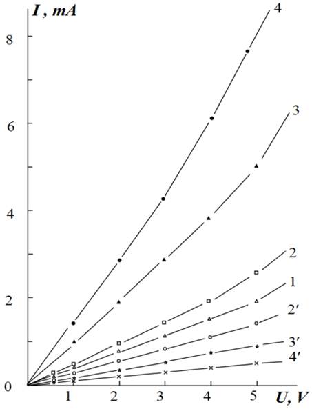
Fig. 1. Current‒voltage characteristics (Bi0.3Sb0.7)2Te3 film on a substrate of polyamide PM-1, under the influence of static deformation: ε×103=0 (a curve 1), 0,3 (2), -0.3 (2´), 0,6 (3), -0.6 ( 3´), 0,9 (4), -0.9 (4´). Curves 2-4 are removed at compression, 2´-4´- at a stretching. Т=300 K.
The results of studying the I‒V characteristics of (Bi0.3Sb0.7)2Te3 films subjected to ASCs are presented in Fig. 2. One can see that the I‒V characteristic of a film changes significantly after N=5×10⁵ cyclic deformations. All curves, recorded at different strains ε, exhibit a pronounced increase in the film resistance and threshold voltage Vth, at which the I‒V characteristic becomes nonlinear. For a film subjected to N=5×10⁵ alternating stress cycles, Vth increases (in the absence of strain in the film) to (10¸12) V (compare curves 1 in Figs. 1 and 2), i.e., by a factor of almost 2‒3. Since cyclic deformations increase the distance between crystallites (because of the wear of contacting surfaces) and the pore size, the linear portion of the I‒V characteristic expands to voltages of (8-10) V under compression (Fig. 2, curves 2‒4) and (12-14) V under extension (curves 2'‒4').
Naturally, tensometric measurements must be performed within the linear part of the I‒V characteristic. The allowable current through a resistance strain gauge must be an order of magnitude lower than the current at which the mechanism of electrical conductivity of the film changes or the strain gauge starts being heated. This current can roughly be estimated from the I‒V characteristic. Generally, this is the current at which the I‒V characteristic begins to deviate from a linear dependence, which can clearly be seen in Figs. 1 and 2.
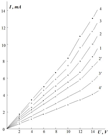
Fig. 2. Current‒voltage characteristics (Bi0.3Sb0.7)2Te3 film after influence N=5×10⁵ of ASCs. Curves 1-4 and 2´-4´correspond to curves 1-4 and 2´-4´; on Fig. 1.
Static deformational characteristics of the films before and after influence of cyclic sign-variable loading in considerable quantities N=5×10⁵ are given in Fig. 3. It is visible that before influence of deformation cycles, resistance of the film almost linearly is increasing under the influence of stretching deformation, while the dependence of resistance on compression deformation are nonlinearly, and the dimension of the coefficient tensosensitivity at stretching deformation is (a curve 1). After the influence of deformational cycles the nonlinearity of the static deformation characteristics of films is decreasing, its tensosensitivity at deformation compression is increasing, and at a stretching is falling (a curve 2), i.e. the asymmetry practically is disappearing.
The dependence of relative change of the resistance ΔR/R on number of cycles of deformation at its different amplitudes ε is given in Fig.4. It is visible that with increasing in number of cycles of sign-variable deformation and its amplitude relative change of resistance isgrowing and the tendency to saturation is observedat values N=5×10⁵ in dependence R(N) (a curves 1-4).
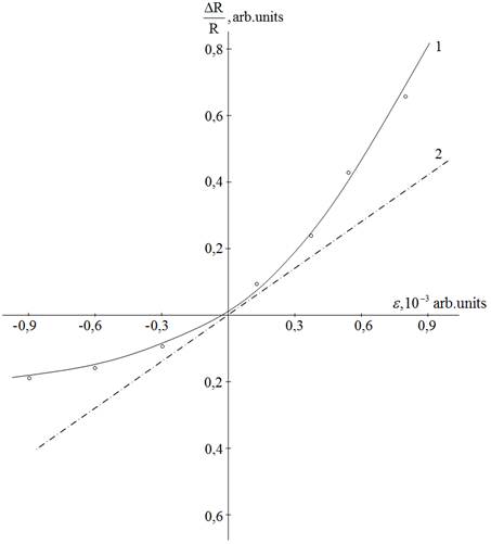
Fig. 3. The deformational characteristic of relative change of resistance films from (Bi0.3Sb0.7)2Te3 before (a curve 1) and after (2) cyclic deformation. N=5×10⁵ for a curve 2.
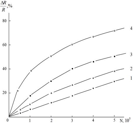
Fig. 4. Relative change of resistance tensofilm (Bi0.3Sb0.7)2Te3 from number of cycles of sign-variable deformations N, at different amplitudes of relative deformations ε×103=±0.25 (a curve 1), ±0.5 (2), ±0.75 (3), ±1.0 (4).
In our opinion, the received experimental facts here can be
explained on the basis of the film model as the systems from micro contacting spending grains of the dielectric backlash between the mare changing with deformation [11, 12]. Really, after the influence of necessary quantity of cycles of sign-variable deformation the width of a backlash between crystal grains is increasing as a result of attrition contacting surfaces of the grains, resistance of the film leading to growth and removal to some extent preliminary internal mechanical stress. The last, it causes aspiration to linear and symmetric kind of deformation characteristic of the film at action of cycle deformation.
3.2. Influence of ASCs on the Temperature Dependence of Film Resistance
Tensometric measurements are performed in different ranges of temperatures of the object under study and its environment. To reduce the measurement error of strain gauges, one must minimize (in magnitude) their temperature coefficient of resistance (TCR) and the temperature strain sensitivity coefficient (TSSC); these characteristics are given by the formulas
a=dR/R0dT, a¢=dK/K0dT, (1)
where R0 and K0 are, respectively, the resistance and strain sensitivity coefficient at a temperature T=273 K in a specified mechanical state of films. A study of these parameters of semiconductor strain gauges should gain a deeper insight into the nature of the physical processes occurring in an inhomogeneous structure (loose polycrystalline film) subjected to mechanical deformation [5].
The temperature dependence of the tensometric parameters of (Bi0.3Sb0.7)2Te3 films was investigated in the range of 293‒455 K. The films obtained at high substrate temperatures (Ts=413) K and high condensation rates (W»400 Å/s) were found to be denser and have low strain sensitivity coefficients. The resistance of these films exhibited a metallic temperature dependence (a=0.85×10⁻⁴ K-1) and barely changed after ASCs (curve 1' in Fig. 5).
Curves 1‒6 in Fig. 5 are the temperature dependences of the resistance of a porous film (K>103), recorded before (curve 1) and after (curves 2‒6) exposure to cyclic deformation. There is a portion with a minimum resistance, Rmin(Tmin), in the temperature range of 293‒413 K. With an increase in the number of alternating stress cycles, this portion shifts to higher temperatures. For example, before the cyclic deformations, Tmin=333 K (point A in curve 1). After the exposure to 1.105, 2.105, and 5.105alternating stress cycles, this portion shifted to the right, and the corresponding temperature values were Tmin= 348, 363, and 408 K (points B, C, and F in curves 2, 3, and 6, respectively).
Thus, when the displacement of the minimum-resistance portion in the temperature dependence R(T) is known, one can estimate the number of alternating stress cycles; i.e., film elements can be applied directly as detail fatigue sensors.
Figure 5 shows that the film resistance first decreases with an increase in temperature (a<0); then passes through a minimum (a=0); and, finally, starts increasing (a>0). The deformation cycles not only shift the position of temperature minimum Tmin for curves 2‒6 to higher temperatures; the film TCR also changes significantly. With an increase in N, temperature Tmin monotonically increases and tends to a constant value, whereas TCR monotonically decreases from a=-5.6×10⁻³ K-1 at N=0 to a=-2.5×10⁻⁴ K-1 at N=5×10⁵.
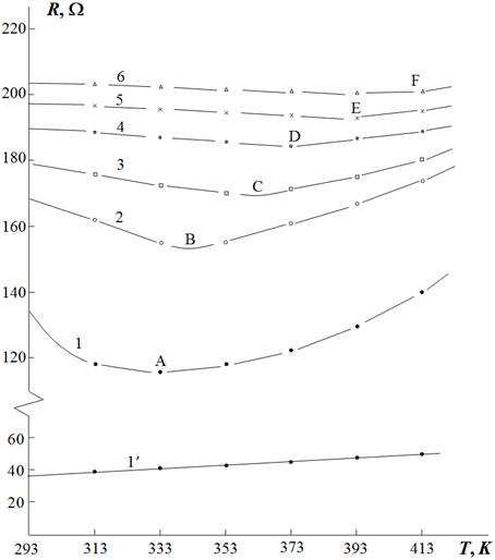
Fig. 5. Temperature dependence of resistance of (Bi0.3Sb0.7)2Te3 films, received on polyamide substrates at temperatures (Ts =413) K (a curve 1´) and (Ts =363) K (1-6) before (a curve 1) and after influence of cyclic deformations: for curves 2-6, N×10-5=1; 2; 4 and 5, accordingly.
The temperature dependence of the film resistance and its change as a result of alternating cyclic deformation can be described qualitatively based on the model representation [3, 5‒7, 9, 10], according to which the film resistance is considered as a set of resistances of intercrystallite gaps, Rpor.i, and separate crystallites, Rcr.i , connected in series:
Rf =Si (Rcr.i+Rpor/i)=Rcr+Rpor. (2)
The component of the film resistance that is due to crystallites, Rcr , depends on temperature as
Rcr=Rcr.0(1+acr×(T-T0)). (3)
This dependence is typical of metal resistors made of a bulk single crystal (Rcr/0 is the resistance of a dense film at T0=273 K).
For a film obtained under optimal conditions (Ts =363 K, condensation rate W=200 Å/s), the micropores (interfaces) along the electric current direction have rather small linear sizes: dpor≤(30-50) Å [3, 7]. They form micropotential barriers with a finite width dpor and energy height Epor for electrons. The current through these barriers is generally determined by the tunnel or over-barrier (Schottky) mechanism. Correspondingly, the film resistance caused by the presence of pores (potential barriers)will change with temperature as
Rpor» Rpor.0×exp(Epor/kT), (4)
where Rpor.0 is some characteristic resistance (weakly dependent on temperature) of the porous film and k is the Boltzmann constant.
With allowance for (2)‒(4), the temperature dependence of the porous film resistance can be written as
Rf (T)=Rcr.0(1+acr×(T-T0 ))+ Rpor.0×exp(Epor/kT). (5)
The temperature coefficient of the film resistance will be determined according to (1) and (5):
af =(acr×Rcr.0 - Epor.Rpor(T)/kT2)/(Rcr.0+ Rpor.0). (6)
Indeed, in correspondence with the data in Fig. 3, it follows from (6) that, if, e.g., the condition acr×Rcr.0< Epor.Rpor(T)/kT2 is satisfied at T=T0, the film first has a negative TCR, which monotonically decreases with an increase in temperature; it turns to zero at some value Tmin and then changes sign. Based on (6), we find that Tmin can be determined from the transcendental formula
Tmin=(Epor ×Rpor(Tmin )/kacrRcr.0)1/2 (7)
or approximately from
Tmin=(Epor ×Rpor(T0)/kacrRcr.0)1/2. (8)
The Epor, acr, and Rcr.0 values are barely affected by alternating cyclic deformation, and the resistance of intercrystallite regions Rpor(T0) increases with an increase in N. Therefore, in correspondence with Fig. 5 and formula (8), the Tmin value increases as Tmin~(Rpor(T0,N))1/2 and tends to a constant at large N=5×10⁵ (see points A, B, C, D, and F in curves 2‒6).
4. Conclusions
The TCR value of the films under study in the temperature range Т < Tmin is mainly determined by the temperature dependence of the film resistance (caused by the highly inhomogeneous film structure). At Т > Tmin, this parameter is determined by the temperature dependence of the resistance of film crystallites (i.e., the bulk material). Under deformation cycles, the dielectric interlayers become thicker as a result of wear of contacting crystallites, thus increasing the Epor and Rpor values and, therefore, changing the position of Tmin in the temperature dependence of resistance.
In addition, we should note that porous polycrystalline films of narrow-gap ternary compound (Bi0.3Sb0.7)2Te3 can successfully be used as FDA sensors in the temperature range T=273-413 K for a number of ASCs in the range of N=0-5×10⁵.
References


