| 1. | ||
| 2. | ||
| 3. | ||
Silicon Nanomaterial Technologies for Detections of Viruses in the Environment
Yuriy Vashpanov1, 2
1Department of Automation of Production Processes and Robotics, Odessa National Academia of Food Technology, Odessa, Ukraine
2Electrical and Computer Engineering Division of Hanyang Institute of Technology, Hanyang University, Seoul, South Korea
Email address

Citation
Yuriy Vashpanov. Silicon Nanomaterial Technologies for Detections of Viruses in the Environment. AASCIT Journal of Nanoscience. Vol. 3, No. 1, 2017, pp. 1-6.
Abstract
Our aim is a searching for specific electrical responses of silicon nanomaterials under loading of NEPO viruses of plant. We used mesoporous silicon and DG MOSFET nanotransistors on the basis of silicon nanowires with the modified surface for detecting of viruses nanoparticles less than 30 nm. Electronic properties of the studied viruses have been observed and discussed. Such researches could be a key for understanding physical properties of "living" matter (virus particles). This result can be useful for creating new biosensors for other similar viruses in the environment.
Keywords
Silicon, Semiconductor Nanotechnology, Biosensors, Viruses
1. Introduction
Silicon is the most well-known and a researched material of semiconductor electronics. Currently, a geometrical dimension of silicon semiconductor devices is approaching to a ten nanometer range. The semiconductor nanostructures have fundamentally new physical properties [1] compared to their massive analogues. Use of nanomaterial based on silicon nanotechnologies (nanowires, nanoparticles, meso- and nanoporous silicon, conical nanocrystal silicone structure) remains as the research object of many laboratories [2-5]. A new silicon material silicene (an analogue of grapheme) is discovered and investigated for field-effect transistors recently [6]. Today the silicon technology for a manufacture of electronics devices is well developed and allows integration the new generation silicon sensors with modern electronic integrated circuits for a signal processing and transmission over wired and wireless computer networks. It makes the indisputable advantage of silicon-based biosensors now.
Particles of viruses are the most interesting and mysterious biological nanomaterial. A surprising property of the virus is a paradoxical stability that is very important for their experimental study. Also the surface of the virus has surfactants with considerable force of surface tension under adsorption. Virus is able to break easy the living cell membrane. A lot of viruses are found till now. We find constantly in recent scientific reports information about new viruses, for example, such as a Zika virus [7]. Early diagnosis for malicious viruses and numerous pathogens and toxins is acquired now paramount. Detection and research of properties of viral nanoparticles more detail became possible as a result of the achievements of nanotechnology methods.
Modern silicon nanotechnologies find applications not only in the electronics industry, but also in medicine, microbiology, chemistry [8-11]. The scientific direction for nanobiosensors technology is formed now [12]. The based on silicon semiconductors nanosensors have a high sensitivity to adsorption by biological macromolecules, viruses [13-16]. Also silicon atoms good absorb organics molecules and play an important role in living organisms. Environment and human food may contain a variety of pathogens which cause various diseases in humans. A develops of nanotechnology for creating of new nanobiosensors for solutions to human security problems is the most urgent area of science today [17]. Silicon semiconductor nanotechnologies have advantages over other diagnostic methods because could be created intellectual electronics device with fast response, with networks for data transmission and for a price low. Considering the primary importance of viruses’ detection in medicine the main purpose for biosensors is to reduce the time of analysis from days to minutes.
Modern biosensorics focused on process automation timely and fast detection of toxic components, since the microbiological diagnostic methods remain laborious and expensive. Biosensors technology is a multidisciplinary science [18], because it requires the integration of disciplines, such as physics, electronics, surface chemistry, biochemistry, microbiology, and medicine. World market of biosensors expects the highest annual growth according to the global strategic business report [19] in the near future. It evidences the high relevance of the chosen research topic.
Nanotechnologies are the most suitable for a food safety, because biosensors could be monitored any falsification during prolonged storage products. Such semiconductors devices have already a great success in the study of molecular interactions, in the detection of pollutants, toxins and antibiotic residues in the food technologies [20]. Now many companies are investing in researches of biosensors as a reliable toosl for quick and inexpensive controls [21]. Silicon-based systems of Lab-on-a-Chip technology [22] is currently popular in rapid diagnostic tests, and is approaching to a large-scale industrial practical using.
Geometrical dimensions of nanomaterials (0.1 nm<d<100 nm) comparable with the dimensions of biological macromolecules, viruses, plants and animal number (dÎ 2….100 nm) (Figure 1). Nanoscale materials change specific electrical, optical, magnetic, mechanical properties by interaction with particular biological substances [23].
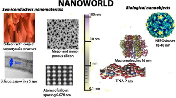
Figure 1. The geometric dimensions of silicon semiconductor nanomaterials and biological macromolecules and viruses.
It should be noted from Figure 1 that the geometrical dimensions of the mesoporous silicon and electronics devices on the base of silicon nanowires correspond to the particle sizes 18-40 nm of numerous viruses. This fact is favorable to researches and development of sensors technology on the base of silicon nanomaterials for such viruses.
2. Experimental Section and Discussion
Porous silicon for this study was formed by anode electrochemical etching of (111) oriented p-type silicon wafer within a resistivity of 10 Ωcm at a current density of 10 mA/cm2 using HF-based solution. During etching an additional illumination and an ultrasonic processing was applied to the silicon surface. A thin metal film on a surface of porous layer was manufactured for a gas and light transparent electrical contact. The technology is described in details in [24].
We was reported about a tunneling mechanism to charge transport mesoporous silicon with columnar structure at a number of loaded nanoparticles plant viruses at room temperature under condition of coincidence of the pore size with the smallest viruses of plant [25]. Figure 2 (curve 1) shows the presence of the tunneling current in the adsorption of virus particles only when the applied voltage is greater than 5 V. The tunnel current was defined by the Fowler-Nordheim theory: ![]() , where
, where ![]() ,
, ![]() ,
, ![]() is the electric field strength,
is the electric field strength, ![]() is Planck's constant,
is Planck's constant, ![]() is the effective height of the tunnel barrier,
is the effective height of the tunnel barrier, ![]() is electron charge and was plotted in specific coordinates
is electron charge and was plotted in specific coordinates ![]() (
(![]() ). The presence of the tunnel current has not been established for macromolecules in our experiments (a curve 2 of Figure 2).
). The presence of the tunnel current has not been established for macromolecules in our experiments (a curve 2 of Figure 2).
The physical mechanism is connected with the formation of tunnel conductive channels between the columnar structures of the porous material through a virus particle. Figure 3 illustrate a difference in mechanisms of adsorption between the protein macromolecules and virus particles. At a virus adsorption in porous space under matches the geometric dimensions of viruses and pores could be formed two contact points of the virus surface (points A and B, on Figure 3). In this case of macromolecules we have an adsorption with one point of contact between the macromolecule and the semiconductors surface (point C, figure 3). A feature of viruses of plant is the presence specific protuberances (glycoprotein spikes) with surfactants, which can hold the virus on the surface of semiconductors well. The glycoprotein spikes can be lengthened that allow the virus to contact the silicon surface under a variation of pore sizes. Compared with macromolecules particles viruses can create more molecular contacts on the surface due to its numerous protuberances. This is particularly important for the formation of two or more contacts between two conductive surfaces of adjacent strands and the formation of conduction channel through viruses. In this case we can investigate the electrical properties of viruses.
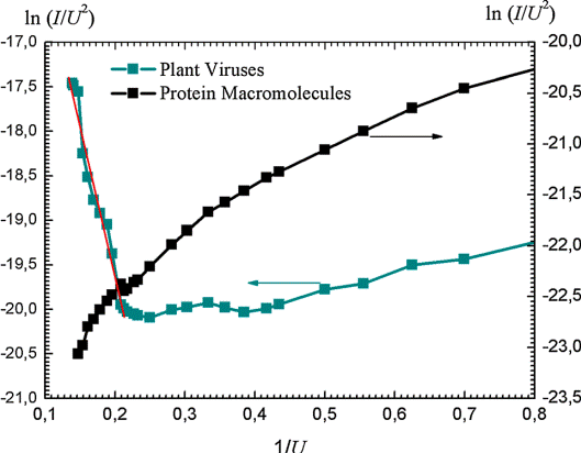
Figure 2. Dependence of the current in the semiconductor structure at a loading of viruses and protein macromolecules in coordinates ![]() (
(![]() ).
).
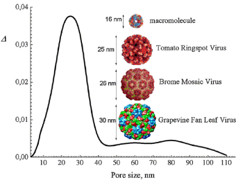
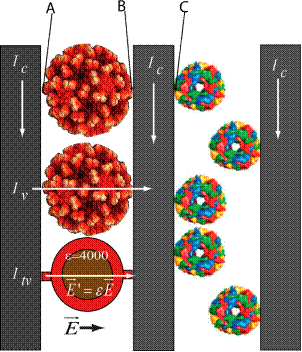
Figure 3. Adsorption mechanisms of viruses and macromolecules at their loading into the porous space.
The adsorption effect between the two nearby situated columnar structure in porous silicon under the viral particles can be understood. The physical reason for the tunnel current through the virus particles may be associated with an increase in their internal electric fields due to the large effective dielectric constant (e»4000) [26]. Thus, the local electric field can be increased to 4000 times (Figure 3). In this case, the electric fields in the samples with a length between contacts l=1 mm under voltage 5 V В equals E=50 V/cm. Electric fields in virus particles with a size of about 30 nm can be achieve 2´104 V/cm (Fig. 3). The effective width of the formed by a virus tunnel barrier limited their characteristic size dv. The effective height of the tunnel barrier f0 should describe by the specific parameters of the virus. Apparently, the transport through the tunnel viruses occurs via long-dimensional circuit consisting of a series of tunnel-transparent barriers. A change of the geometrical and electronically properties may lead to changes in the parameters of the effective potential barrier that observed experimentally.
We can find the barrier height, if we will numerically differentiate an experimental data. Figure 4 shows calculations results for barrier height f0 in depending of the applied voltage for the smallest TORSV, GVA, GFLV viral particles. The increase in voltage results in a non-linear increase in the height of the barrier for the investigated virus particles. Thus, viral particles change their electrical properties depending on the applied voltage and have a non-linear response. We can only estimate the effective magnitude of the tunneling barrier, assuming that it is equal to the effective width dv. However, it still requires additional refinements and more detailed studies. The obtained experimental data can be used for identification and characterization of viral particles.
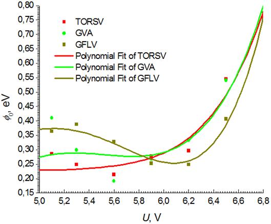
Figure 4. Electrical properties of the smallest TORSV, GVA, GFLV viruses under different voltages.
Investigated viruses are the smallest among the numerous viruses. Samples of porous silicon have a narrow pore size distribution. Experimentally, it is important to make a porous material with pore size comparable to the size of virus particles to be detected. In practice this is not always easy. There are a lot of viruses with similar and larger dimensions than plant viruses. The proposed method is based on the presence of the electrical effect between the fibrous structures of the mesoporous silicon is the most simple method for environmental studies for the presence of pathogenic viruses. The applicability of the method to relatively large viruses such as Papillomavirus (460 nm) is not so obvious. It is necessary to check the entire spectrum of viral particles to find the size of the upper limit that can be detected by the proposed method.
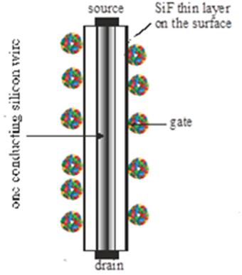
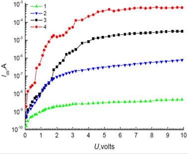
Figure 5 (a) shows a 3D technology DG MOSFET nanotransistor on the base of silicon nanowires and electronic characteristics of nanoparticles with biological adsorption (b).
a)
b)
Figure 5. 3D technology DG MOSFET nanotransistors on the base of silicon nanowires (a) and electronic characteristics when loaded biological nanoparticles (b) [27].
Simulation of the gate-drain characteristics of DG MOSFET nanotransistors and their comparison with experimental data is important. For a description of current flow, we used the formula: ![]() , and
, and ![]() . The parameter
. The parameter ![]() is a solution of equation:
is a solution of equation:
![]() ,
,
where ![]() is the charge of an electron,
is the charge of an electron, ![]() is the Boltzmann constant,
is the Boltzmann constant, ![]() is the absolute temperature,
is the absolute temperature, ![]() is the dielectric constant of crystalline silicon,
is the dielectric constant of crystalline silicon, ![]() ,
, ![]() are the width and length of the channel,
are the width and length of the channel, ![]() is the silicon nanowire thickness,
is the silicon nanowire thickness, ![]() is the effective mobility of silicon, Df - the difference of potential energy in the gate,
is the effective mobility of silicon, Df - the difference of potential energy in the gate, ![]() amd V are voltages on the gate and between the source and drain,
amd V are voltages on the gate and between the source and drain, ![]() is the concentration of charge carriers in silicon and
is the concentration of charge carriers in silicon and ![]() is a structural parameter of the electronic device.
is a structural parameter of the electronic device.
Transistors based on silicon nanowires take the form of a coaxial cylinder, the capacity of which can be estimated by the formula: ![]() , where e0 is the vacuum permittivity. The capacitance value for the inner radius
, where e0 is the vacuum permittivity. The capacitance value for the inner radius ![]() = 5÷25 nm, dielectric thickness d= 2÷5 nm, length L= 100÷500 nm and dielectric constant e =4.5 is in limit 1.2÷27 nF. In the line mode of the DG MOSFET transistor, we can find the number of the adsorbed particles, which can be estimated from the relationship
= 5÷25 nm, dielectric thickness d= 2÷5 nm, length L= 100÷500 nm and dielectric constant e =4.5 is in limit 1.2÷27 nF. In the line mode of the DG MOSFET transistor, we can find the number of the adsorbed particles, which can be estimated from the relationship ![]() . With the help of Matlab programs were found numerically correlations b and
. With the help of Matlab programs were found numerically correlations b and ![]() with different geometrical and electronically parameters of our device. We were modeling the relationship between the number of adsorbed particles and the drain current under variation of the transistor parameters. Figure 6 shows the dependence
with different geometrical and electronically parameters of our device. We were modeling the relationship between the number of adsorbed particles and the drain current under variation of the transistor parameters. Figure 6 shows the dependence ![]() for the case
for the case ![]() = 25 nm, d= 5 nm, L= 500 nm. As can be seen from Figure 6 DG MOSFET transistor by these parameters already has sufficient sensitivity to detect single particles.
= 25 nm, d= 5 nm, L= 500 nm. As can be seen from Figure 6 DG MOSFET transistor by these parameters already has sufficient sensitivity to detect single particles.
Figure 6. Dependence of the current DG MOSFET transistors based on silicon nanowires with the parameters ![]() = 25 nm, d== 5 nm, L = 500 nm from the number of adsorbed particles.
= 25 nm, d== 5 nm, L = 500 nm from the number of adsorbed particles.
3. Conclusions
Researches of the electrical properties of viral particles could be a key for understanding their biochemical and physical properties. Our experimental method for studying the electrical properties of the viruses of plant with the mesoporous silicon is opening a new way for such researches. Studies of the internal mechanism of the electrical transport through the viral particles and detection of their specific electrical parameters create a new direction of nanobiophysics, because the electronic properties of the viruses hardly studied. The non-linear electrical responses of viruses may be associated with specific changes in the "living" matter (viral particles) and can serve as a simple method of their identification. DG MOSFET transistors based on silicon nanowires with modified surface can effectively be used as a biological sensor nanoparticle (macromolecules, viruses, particles less than 30 nm). Our results show that nanotechnologies with the silicon nanomaterials are keeping a good potential for researches of the biological nano-matter and the biosensors today.
References


