| 1. | ||
| 2. | ||
| 3. | ||
| 4. | ||
Optical Investigations of Bulk Heterojunction Blend (NiPcTs/PEDOT:PSS) Thin Films
Morooj A. Abood1, Ameer F. Abdulameer1, Izzat M. AI-Essa1,
Falah I. Mustafa2, *
1Physics Department, College of Science, Baghdad University, Baghdad, Iraq
2Solar Energy Research Center, Renewable Energy Directorate, Ministry of Higher Education and Scientific Research, Baghdad, Iraq
Email address
 (M. A. Abood)
  (A. F. Abdulameer)
  (I. M. Al-Essa)
  (F. I. Mustafa)
 Citation
Morooj A. Abood, Ameer F. Abdulameer, Izzat M. AI-Essa, Falah I. Mustafa. Optical Investigations of Bulk Heterojunction Blend (NiPcTs/PEDOT:PSS) Thin Films. AASCIT Journal of Materials. Vol. 2, No. 2, 2016, pp. 6-11.
Abstract
Thin films of bulk heterojunction blend Ni-Phthalocyanine Tetrasulfonic acid tetrasodium salt and poly (3,4-ethylenedioxythiophene) poly (styrenesulfonate) (NiPcTs/PEDOT:PSS) with different (PEDOT:PSS) concentrations are prepared by using spin coating technique with thickness 100nm deposited on pre-cleaned glass substrate. The variation in films absorption and optical energy gaps were studied at room temperature using UV-Visible spectra. The decreasing amount ofPEDOT:PSS concentration, leads to increase optical absorbance of films with peak shifts position to high wave lengths side of wavelength spectra. The optical energy gap range of (NiPcTs/PEDOT:PSS) thin film between (1.7-1.9)eV for Q-band and (2.9-3.3)eV for B-band with direct energy band. The optical energy gap obtained fromphotoluminescence spectra for NiPcTs/PEDOT:PSS bulk heterojunction blend thin film with supply excitation wavelength 315 nm is very approach to energy gap obtained by UV-VIS spectrum. FTIR measurements for these bulk heterojunction blend thin films also carried out in this work and obtain good information about the bonds and their locations.
Keywords
Organic, Semiconductor, Phthalocyanines, Optical Properties
1. Introduction
Organic semiconductors are a class of materials that combine the electronic advantages of semiconducting materials with the chemical and mechanical benefits of organic compounds such as plastics. Thus, that have ability to absorb light, conduct electricity, and emit light is united with a material structure that can easily be modified by chemical synthesis, for example, to tailor electronic properties such as the desired emission wavelength, to render it soluble, or to allow for mechanically robust, lightweight, and flexible thin films [1].
There are two major classes of organic semiconductors: low-molecular weight materials and polymers for an overview see reference [2]. An important difference between the two classes of materials lies in the way how they are processed to form thin films. Whereas small molecules are usually deposited from the gas phase by sublimation or evaporation, conjugated polymers can only be processed from solution, example by spin coating or printing techniques [3]. Organic semiconductors have attracted much attention due to their successful application in optical and electronic devices with encouraging performances.
The formation of charge carriers under the action of light is due to the decay of excitons on the surface of the crystal, at structural defects, and at impurities when exciton interaction occurs; it may also be due to the auto ionization of highly excited molecules. The conduction bands are narrow (~0.1 electron volt), and the mobility of the charge carriers is generally low (~1cm2/volts). In addition to the band mechanism of electrical conduction, the hopping mechanism may operate. In crystals of ion radical salts; the intermolecular interaction is strongly anisotropic.
For this reason, the optical and electrical properties are highly anisotropic, and such organic semiconductors can be regarded as quasi-one-dimensional systems [4, 5]. Organic heterostructur photovoltaics have attracted significant interest due to their potential for inexpensively generating electricity. Substantial work has recently been done to simulate numerically layered organic heterojunctions in order to describe the exciton creation and the dissociation at a donor–acceptor interface, the predominant channel of exciton dissociation [6, 7]. Blending of polymers has long been established as a technique to tune their physical properties. Often the blend can be designed to combine attractive features of both components, and sometimes the microstructure of the blend has new properties not present in either component. In the field of polymer electronics, where conjugated polymers are processed from solution to form the active semiconducting layer of a light-emitting diode (LED) or photovoltaic device, blending is an attractive approach to optimize the device function. Indeed for photovoltaics the presence of heterojunctions between two different semiconductors (donor and acceptor) is vital to dissociate the excitons produced by photo excitation. In a polymer-blend LED, the two component scan be chosen to give efficient injection of electrons and holes at opposite electrodes, with recombination occurring at or close to the heterojunction. [8] Semiconductors Phthalocyanines are a class of highly stable organic semiconductors and have attracted much attention because of their low cost and little toxicity [9, 10] and have good sensitivity and selectivity [11] widely used for sensor applications and transistor fabrication, which has excellent stability against heat, light, moisture and oxygen [12]. The physical properties are controlled by traps, which are associated with dislocations, imperfections, grain boundaries and surface topology of film [13]. PEDOT, poly (3,4-ethylenedioxythiophene) [14], is a conductive polymer [15] that can be used in many different applications such as antistatic coating of polymers and glass, high conductive coatings, organic LED-(OLED) displays, nano-fiber electrodes for cell stimulation, solar cells, cathode material in electrolytic capacitors, printing wiring boards [16], textile fibers with color changing properties [17], transparent electrodes for thick-film electroluminescence [18], source gate and drain in the rapidly developing organic semi-conductors field In the field of polymer electronics, where conjugated polymers are processed from solution to form the active semiconducting layer of a light-emitting diode (LED) orphotovoltaic device, blending is an attractive approach to optimizethe device function. Indeed for photovoltaics the presence of heterojunctions between two different semiconductors (donorand acceptor) is vital to dissociate the excitons produced byphotoexcitation. In a polymer-blend LED, the two component scan be chosen to give efficient injection of electrons and holes at opposite electrodes, with recombination occurring at or close to the heterojunction. In both cases, it is important that both electrons and holes can be transported on the respective components of the blend, either from the heterojunction to the relevant electrode, or vice versa. This places considerable constraints on the microstructure that is required [19]. Bulk heterojunctions formed by an interpenetrating blend of an optically active polymer and electron accepting molecules constitute a very promising route toward cheap and versatile solar cells [20].
2. Experimental
The p-type organic semiconductors NiPcTs and PEDOT:PSS were obtained from Sigma-Aldrich without more purification. Fig. 1 shows the structure of the NiPcTs and PEDOT:PSS molecules. NiPcTs was dissolved in dyonoyiz water and mix well using magnetic stirrer to be homogeneous then was prepared the three concentrations of PEDOT:PSS (0.5, 1 and 2). The silde glasses were cleaned by distilled water then acetone and alcohol. The thin films deposited using spin coater with 100nm thickness at room temperature, the spin rate was 1500rpm for time 1.5min on glass substrate. The optical measurements include UV-Visible, Photoluminescence (PL) and Furrier Transform-Infra Red (FTIR). UV-VIS (Spectrometer-2601) with scan range (190-1100nm) to examine the absorbability, Photoluminescence measurements recorded by single beam spectrometer for NiPcTs/PEDOT:PSS thin films To show the role of traps PL measurements have been done at exciting wavelength 312nm and (FTIR TENSOR 27) (400-4000 cm-1) to find out the nature of the bonds with the compound.
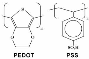
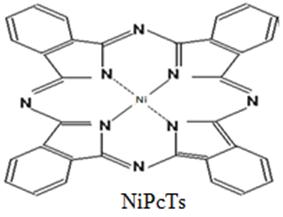
Fig. 1. Molecular structure of the NiPcTs and PEDOT:PSS molecules.
3. Results and Discussion
The absorption and transmition spectra of NiPcTs/PEDOT:PSS bulk heterojunctions blend thin films of thickness 100nm deposited with different PEDOT:PSS concentrations are given in the figure 3. Show that Q and B bands shift towards longer wavelength with decreasing the concentrations PEDOT:PSS and shift towards shorter wavelength side when increasing the concentrations of PEDOT:PSS. It is also observed that the intensity of absorption maxima observed at (1,0.5) concentrations. But the highest transmission at concentrations (2) PEDOT:PSS, this explains that use PEDOT:PSS in the manufacture of solar cells.
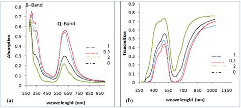
Fig. 2. (a). Absorbance and (b) transmittance as a function of wavelength for NiPcTs/PEDOT:PSS bulk heterojunctions blend thin films of different PEDOT:PSS concentrations.
Fig 3. Shows the direct energy band gaps obtained UV-Visible spectra of NiPcTs/PEDOT:PSS bulk heterojunctions blend films. The direct energy gaps values are listed in the Table (1) which show that the energy gap increase with increasing concentrations of PEDOT:PSS.
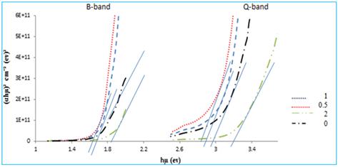
Fig. 3. (αhʋ)² versus photon energy of incident radiation for different concentration.
Photoluminescence spectrum or emission spectrum has great importance since it gives information about the optical energy band gap, excitons and traps energy levels. The energy gap value that has been obtained from photoluminescence spectrum is more accurate than that calculated by Tauce equation. The photoluminescence spectra for NiPcTs/PEDOT:PSS bulk heterojunction blend thin films of different concentration are shown in Figure (5) and the optical energy gap values are tabled in table (1) with excitation wavelength 315 nm, compared with Eg found by Tauce equation. We can see that the lowest value for Eg is at Concentration 0.5. Figure also shows the intensity higher in Concentration (1) of PEDOT:PSS.
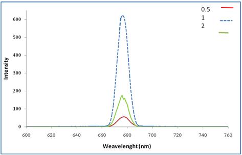
Fig. 4. Photoluminescence spectra for NiPcTs/ PEDOT:PSS bulk heterojunctions blend thin films at different concentration.
Table 1. The optical band gap energies of NiPcTS: PEDOT:PSS bulk heterojunctions blend thin films of thickness 100 nm deposited at different concentrations at room temperature.
| Direct Energy gap (Tauce) (eV) | Energy gap (PL) (eV) | Concentrations of PEDOT:PSS | |
| B-Band | Q-Band | ||
| 1.77 | 3 | - | 0 |
| 1.7 | 2.8 | 1.8 | 0.5 |
| 1.75 | 2.9 | 1.82 | 1 |
| 1.85 | 3.3 | 1.85 | 2 |
Fig. 5 shows the FT-IR spectrum for NiPcTs: PEDOT:PSS bulk heterojunctions blend thin films in different concentration was measured at room temperature and compared with NiPcTs spectrum. FT-IR for NiPcTs: PEDOT:PSS thin films shows the bond bending represented by the range (400-2000) cm-1 while the bond stretching represented by the range (2000-4000) cm-1. The spectrum shows a weak peak in the range (600-400) cm-1 which indicate the presence of (metal-Nitrogen) bond vibration at (508-578) cm-1 have been assigned for (Nickel – Nitrogen). A number of well-defined bands assigned to PEDOT vibrations are found in the region of 500 to 2000 cm-1 as depicted and 1400 to 1500 cm-1 associated with C=C symmetrical stretching has been employed to distinguish PEDOT being in its benzoid and quinoid [19]. The band at (1300-1000) cm-1 is for bond of C-O stretching and the peak (1627-1636) cm-1 indicates C=C bond and the peak at (1533) cm-1 indicates Benzene ring band. The band at (3427-3448) cm-1 is for bond of O-H stretching. The spectrum shows the absent of stretching band N-H at band 2359 cm-1 which is appears in 0.5 PEDOT:PSS concentration spectrum.
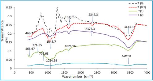
Fig. 5. FT-IR spectra for NiPcTs/ PEDOT:PSS bulk heterojunctions blend thin films of different PEDOT:PSS concentrations.
The scanning electron micrographs of thin films deposited at room temperature, annealed at 100ºC are shown in the Fig. (6). The film morphology changes for increasing the concentrations of PEDOT:PSS. At concentration 0.5 uniform and smooth grain morphology is observed with fibers and When increase the concentration of PEDOT:PSS to 1 more clearly shows the fiber and approaching to nano fibers at Concentration 2.
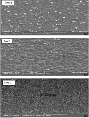
Fig. 6. SEM for NiPcTs/ PEDOT:PSS bulk heterojunctions blend thin films of different PEDOT:PSS concentrations.
4. Conclusions
The NiPcTS/PEDOT:PSS bulk heterojunctions blend as solution and thin films are successfully prepared. The optical characterization of these blend thin films was found that the maximum absorption peak shift towards shift towards longer wavelength with decreasing the concentration of PEDOT:PSS and shift towards shorter wavelength side when increasing the PEDO:TPSS concentration. It is also observed that the intensity of absorption maxima observed at concentration (0.5), while the highest transmittance at (2) concentration in the region of visible that cause increasing of optical energy. The B-band and Q-band indicate the presence of two energy gap, the absorption intensity at both regions has also been varies with concentrations of PEDOT:PSS. The optical energy gap increase with increasing concentrations of PEDOT:PSS. Optical energy gap obtained from photoluminescence spectrum is more similar to the optical energy gap obtained from UV-VIS spectrum. FTIR measurement was applied to know the type of the bonds of NiPcTS/PEDOT:PSS bulk heterojunctions blend thin films.
References


