| 1. | ||
| 2. | ||
| 3. | ||
| 4. | ||
| 5. | ||
Optimization of Timing and Control Circuit for Low Power ROIC Design
Hari Shanker Gupta1, M. Shojaei Baghini1, A. S. Kiran Kumar2, Dinesh K. Sharma1
1Department of Electrical Engineering, Indian Institute of Technology Bombay, Mumbai, India
2Space Applications Centre, Jodhpur Tekra, Ahmedabad, India
Email address
 (H. S.Gupta)
  (M. S.Baghini)
  (D. K. Sharma)
 Citation
Hari Shanker Gupta, M. Shojaei Baghini, A. S. Kiran Kumar, Dinesh K. Sharma. Optimization of Timing and Control Circuit for Low Power ROIC Design. International Journal of Electrical and Electronic Science. Vol. 3, No. 2, 2016, pp. 8-12.
Abstract
Infrared detectors are normally bonded with ROICs using indium bumps. High spatial resolution and large field of view demands for large area ROIC array and reduced pixel size. Pixel size reduction and large number of pixels requirements, increases complexity of supporting read out circuits, interfaces and power demands. The timing and control clocks are required for proper pixel selection and signal processing of pixel information. In general, pixels are sequentially selected and the pixel information is transferred to the ROIC output after necessary processing. The traditional timing approach leads to the requirements of high power budgets for the selection of column amplifier. This paper proposes a timing and control design for column amplifier selection and its power minimization. The technique has been implemented on a test chip of 4×4 ROIC array and achieved 70% reduction in power budget of column amplifiers. The paper will discuss experimental results from the test chip and its estimation for large pixel arrays.
Keywords
Pixel, Pitch, Readout Integrated Circuit (ROIC), Column, Row etc.
1. Introduction
Infrared (IR) detectors are widely used in a large number of commercial, bio-medical, industrial and space applications [1,2,3]. The design of CMOS based Readout Integrated Circuit (ROIC) is necessary due to severe space and power constrains [3]. The space constrains arise from the fact that very little space is available for accommodating the pixel amplifier electronics [3. 4]. The power constraint arises from the operating temperature requirement of the IR detectors which must be kept at cryogenic temperatures [3,5]. The cryogenic cooling requirement is generally met by the use of active coolers/Peltier coolers [5]. These coolers have limited cooling capacity, which puts constraints on the power requirement of the ROIC. ROICs consist of a charge integration stage, charge to voltage converters, correlated double samplers (CDS), sample and hold circuits, column amplifiers, analog multiplexer, and a buffer stage as shown in Fig. 1. Most of the power dissipated in an ROIC is consumed in the pixel and column amplifiers since the pixel amplifiers are repeated of M×N times while column amplifiers are repeated N times (for a detector array with M rows and N columns). Unit cell designs like source follower detector (SFD), direct injection (DI), buffered direct injection (BDI), capacitive trans-impedance amplifier (CTIA) etc are addressed in [1-6].
![]()
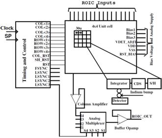
Fig. 1. ROIC Block diagram.
This paper mainly highlights design constraints and optimization aspects of the column amplifier power budget through a timing and control circuit to minimize ROIC power.
2. Column Amplifier Stage
Critical systems like space applications normally require continuous data. The "read while integration" mode (also called the snapshot mode) supports continuous data collection. However it requires a signal processing stage and a hold capacitor to store integration information of the previous frame during integration of the current frame. Other techniques like integrate then read mode of operation loses alternate frame information and is not appropriate for critical systems. Fig. 2 shows the hold capacitor stage of the unit cell design and the column amplifier stage of the readout integrated circuit. The signal from the hold capacitor of the unit cell is sampled onto the column amplifier buffer. Critical parameters of the column amplifier are slew rate, gain bandwidth product, settling time and noise. There are various methods for implementing the column amplifier stage, such as source follower, charge sensitive amplifier (CSA) and master-slaver technology. Major disadvantage of source follower are linearity and column bus parasitic capacitance. Charge sensitive amplifier (CSA) and Master-slaver technology also used in many circuits [2], [3], [4]. The proposed unity gain buffer amplifier based design is a preferred approach for low power implementation [8,9]. The column amplifier design with a unity gain buffer amplifier and additional analog multiplexer is shown in Fig. 2. Choice of unity gain buffer reduces gain and bandwidth requirements of the column amplifier. Typical timing requirements for this are shown in Fig. 3 for 4×4 pixel readout. The pixel information is readout sequentially as illustrated by its timing sequence in Fig. 3.
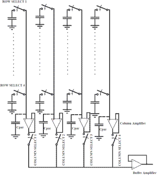
Fig. 2. Unity gain column amplifier approach.
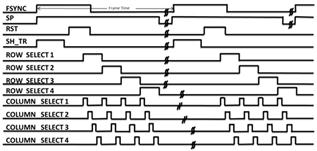
Fig. 3. Typical Timing requirements.
In this methodology, the column amplifier needs to operate at the readout rate and demands more power for each column amplifier [10]. In this timing scheme, the column amplifiers are required to meet precision requirement of better than 14 bit to support a variable frame rate of 100 Hz to 5 KHz. Eqn. 1 shows the accuracy requirement for 14 bit accurate ROIC performance
![]()
![]() (1)
(1)
The settling time TSS can be expressed by
![]() (2)
(2)
Where, N is the required accuracy and settling time
![]()
For N = 14, and
![]()
![]() (3)
(3)
Column amplifiers have to meet critical parameters of DC gain 95 dB (5dB margin for PVT corner variation), gain bandwidth product > 25 MHz with all margins for PVT and layout variation. The power requirements for these specifications are 1mW/column amplifier for a load capacitor of 1pF. The design of 320×256 ROIC needs 256 column amplifiers which leads to the substantial column amplifier power budget of 256 mW.
3. Proposed Low Power Design Techniques
The proposed low power design technique is an efficient implementation of the unity gain column amplifier.
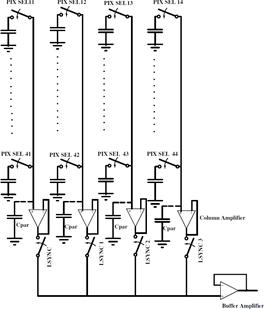
Fig. 4. Proposed design technique.
The timing and control circuit has been optimized for the pipeline column amplifier stages of the ROIC in-order to reduce column amplifier power. The pixel select signal for all pixels has been implemented through simple logical AND operation on the Row select and Column select signal of address decoder. These pixel select signals enable transfer of pixel information from each pixel hold capacitor to column amplifier bus as shown in Fig. 4. The line synchronization clock LSYNC (LSYNC1, LSYSNC2 etc) signals have been introduced for pipelining the ROIC activity as illustrated in Fig. 5. The timing and control circuit generates Row and Column signals based on the detector array requirements. When Row and Column select signal is high, it transfers the corresponding pixel information on to the column bus. The column amplifiers now get a long time to settle. The optimum number for this is (N -2) times the pixel readout time where N (=4 for a 4×4 or 256 for a 320×256 array) is the total number of column in ROIC array. One cycle is used for resetting the column bus before transferring information of next row pixel on the same column bus.
The column bus will have information on the same column line after a full line period. This allows us to slow down the requirements of column amplifier and power minimization. For example the first ROW and first column has been selected by its select signals and transfers pixel information to the corresponding first column line.
![]()
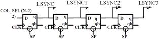
Fig. 5. Proposed timing requirements.
The column bus will have information on the same column line after a full line period. This allows us to slow down the requirements of column amplifier and power minimization. For example the first ROW and first column has been selected by its select signals and transfers pixel information to the corresponding first column line.
The first column now retains the information of first pixel and can settle for a long time up to three clock cycles for a 4×4 array. It reduces the settling time requirement of the column amplifier. It also reduces power requirements of each column amplifier. The worst case time available to column amplifier is a single line period. However this large settling time may have a disadvantage due to drooping effect. We have selected the optimum number (Three for 4×4 array and 16 for 320×256 array) and reduced the column amplifier power requirements. This will be even more effective for a large pixel array. The Power budget has been reduced to 16 mW from 256 mW for a 320×256 ROIC design. Fig. 6 shows circuit implementation for LSYNC as per 4×4 array requirements
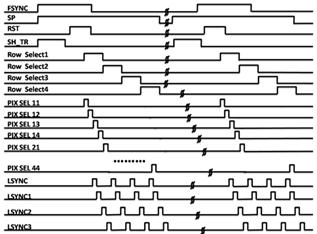
Fig. 6. LSYNC Timing circuit.
The column amplifier requirement for 14 bit precision and variable frame rate of 100 Hz to 5 KHz has been relaxed. Column amplifier to meets critical parameters of DC gain (>95 dB), gain bandwidth product (> 400 KHz). The power requirements for theses specifications are 62µW/column amplifier. We have made a prototype design of a 4×4 array and reduced the power budget of the column amplifier by 70%. The RESET signal is also required for each column line after its information is transferred to the next buffer stage.
The column residual error occurs due to the charge present on the parasitic capacitor at the input of the column amplifier. Hence one very obvious solution is to reduce the parasitic capacitance to its minimum. Careful layout techniques have been used to keep this parasitic capacitance to minimum. However there will still be some minimal parasitic capacitance, whose charge needs to be removed after every read out of the column amplifier. Hence a column reset switch has been incorporated at every column amplifier to reset the charge to the reference voltage.
4. Performance Simulation
The proposed design has been simulated in cadence hspice simulator using 180 nm CMOS process for ROIC input stage, direct injection (DI) type unit cell, column amplifier and buffer amplifiers. We have observed that column amplifier and analog buffer outputs have settled well within for worst case simulation as shown in Fig. 7. The ROIC output has been simulated for two consecutive pixels illuminated with maximum and minimum currents and readout at 5 M pixel per second (Mpps). We have simulated power dissipation of individual ROIC sub-modules. Fig. 8 and Fig. 9 shows significant improvement in the column amplifier power budget due to reduction in the unity gain bandwidth requirements as we have NOW delayed sampling of column amplifier output by LSYNC signal. The ROIC simulation has been executed for uniform illumination and checker board pattern for all pixels. An equivalent electrical model of detector was used for the simulation. Simulation has been performed at various frame rates. Complete analog chain linearity analysis was also performed and found to be within 99.9%.
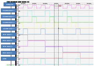
Fig. 7. ROIC Analog Output and other signals for consecutive high/low input signals.
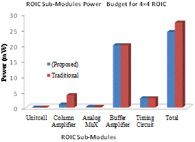
Fig. 8. Power distribution in 4×4 ROIC sub-modules.
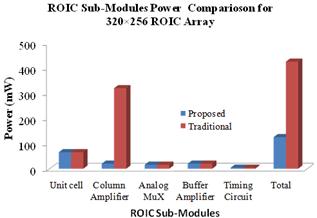
Fig. 9. Power distribution in 320×256 ROIC sub-modules.
5. Experimental Results
The design of various blocks of the ROIC such as unit cell, column amplifier, buffer amplifier with proposed timing and control circuit has been implemented on the 4×4 ROIC chip. Design has been fabricated in UMC 180 nm CMOC process. Various design trade-off have been carried out to get the best possible performance of the unit cell in a limited space of 30×30 µm with minimum power of 25 mW for 4×4 array and 130 mW for 320×256 array size.
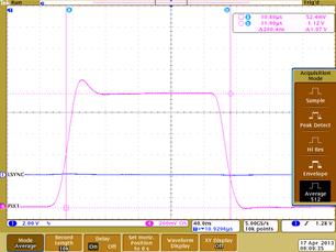
Fig. 10. Analog output of ROIC at 5 MHz pixel rate.
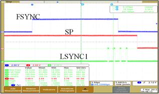
Fig. 11. Line Sync (LSYNC1) Relation with SP.
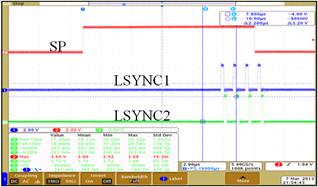
Fig. 12. LSYNC1 & LSYNC2 Relation with SP.
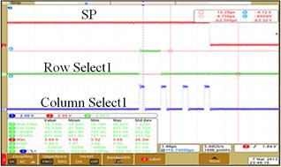
Fig. 13. Clock relation of row and column select.
Table 1. Chip performance summary.
| ROIC Parameters | Measurement Results | [6] |
| Array size (µm×µm) | 4×4 | 8×10 |
| Pixel sixe (µm2) | 30×30 | 30×30 |
| Input cell | DI | CTIA |
| Integration Type | Snapshot | Snapshot |
| Frame Rate | 0.1 to 5 KHz | 110Hz |
| Pixel rate | 5 MHz | 3 MHz |
| Power (mW) | 25@CL= 25pF | 9.1 |
| Charge Handling Capacity (Mē) | 10 | 2 |
| Operating Temperature | 77 to 310K | 77 to 310K |
The post layout simulation and experimental results closely match each other. Pixel output at 5 MHz has been captured and it shows a well settled analog output for given signal level. The error due to residual charge on the column amplifier has been rectified by addition of column reset circuit. Fig. 11 to Fig. 13 illustrates measured timing relation in fabricated device. Detailed performances have been illustrated in Table. 1.
Acknowledgments
The authors acknowledge with thanks to Shri Tapan Mishra, Director, Space Applications Centre, Ahmedabad, India for their support. Authors also acknowledge with thanks to Mr, Sanjeev Mehta, Mr, Sandip paul for their valuable suggestions. We would like to thank Saji A Kuriakose Deputy Director, Space Applications Centre, Ahmedabad, India for their support and VLSI Design Group, IIT-Bombay for insightful discussions
References


